How Gallium Nitride Enables Smaller, More Efficient Power Supplies
How Gallium Nitride Enables Smaller, More Efficient Power Supplies

Gallium Nitride is a wide band-gap semiconductor material, which can be used to make semiconductor devices such as diodes and transistors.
Sponsored by CUI Inc
One of the most common transistors in switching power supplies is a metal–oxide–semiconductor field-effect transistor (MOSFET). While popular, MOSFETs experience losses in the silicon when operating at high switching frequencies. Power designers have begun to turn to GaN as it has become increasingly difficult to increase performance as MOSFETs near their physical limits.
Gallium Nitride (GaN) is a wide band-gap (WBG) semiconductor material, and like silicon, GaN can be used to make semiconductor devices such as diodes and transistors.
A power supply designer would choose a GaN transistor instead of silicon if they were targeting a small form factor and high efficiency. The losses in a silicon MOSFET make their use undesirable due to thermal management requirements, compared to a GaN transistor, which would dissipate less power and more efficiently conduct heat away.
Read More About: Nanomaterials Transform Manufacturing
The development of GaN transistors has been of particular interest to the power electronics industry. As a transistor, GaN shows significant advantages over silicon in critical areas that allow power supply manufacturers to significantly increase efficiency, while at the same time decreasing the size and weight of their devices.
How Does GaN Improve Efficiency?
Power transistors are one of the primary contributors to power loss in a switching power supply. Losses in the transistors are generally separated into two categories: conduction and switching. Conduction losses are those caused by current flow when the transistor is on, and switching losses occur in the transition between on and off states.
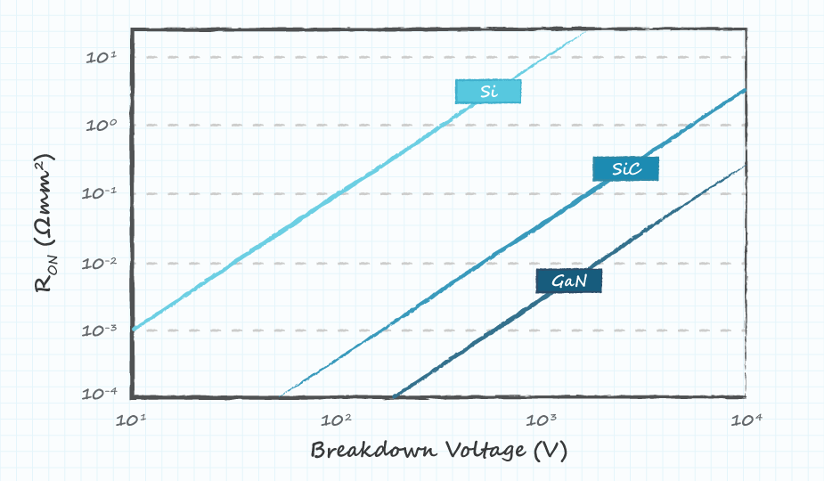 Figure 1: Theoretical limits of resistance between drain and source versus breakdown voltage for Si, GaN, and SiC transistors. Photo: CUI
When on, GaN transistors (like those made of silicon) resemble a resistance between drain and source, often referred to as Ron, and the conduction losses are proportional to this resistance. A key benefit of GaN and other WBG materials is their relationship between breakdown voltage and Ron. Figure 1 shows the theoretical limits of this relationship for silicon, GaN, and silicon carbide (SiC), another WBG material. It can be seen that for a given breakdown voltage, the Ron of the WBG devices is much lower than that of silicon, with GaN being the lowest of the three. As silicon is nearing its theoretical limit, the use of GaN and other WBG materials becomes necessary if improvements to Ron are to continue.
Figure 1: Theoretical limits of resistance between drain and source versus breakdown voltage for Si, GaN, and SiC transistors. Photo: CUI
When on, GaN transistors (like those made of silicon) resemble a resistance between drain and source, often referred to as Ron, and the conduction losses are proportional to this resistance. A key benefit of GaN and other WBG materials is their relationship between breakdown voltage and Ron. Figure 1 shows the theoretical limits of this relationship for silicon, GaN, and silicon carbide (SiC), another WBG material. It can be seen that for a given breakdown voltage, the Ron of the WBG devices is much lower than that of silicon, with GaN being the lowest of the three. As silicon is nearing its theoretical limit, the use of GaN and other WBG materials becomes necessary if improvements to Ron are to continue.
In addition to improvements in conduction losses, the use of GaN also leads to a reduction in switching losses. Multiple factors contribute to switching losses, several of which are improved through the use of GaN. One loss mechanism results from the fact that the current in a FET begins to flow before the drain-source voltage begins to fall, as shown in Figure 2. During this time, the losses (equal to the volt-amp product) are very large. Increasing the speed at which the switch turns on will reduce the losses incurred during this transition. Because GaN transistors can turn on faster than silicon FETs, they are able to reduce the losses caused by this transition.
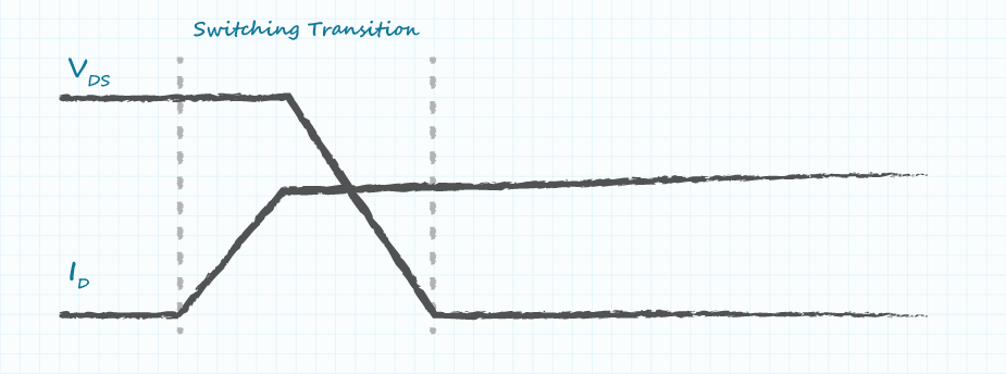 Figure 2: Drain Voltage and current waveforms during switching transition. Photo: CUI
Another way that GaN reduces switching loss is through the absence of a body diode. To avoid a short circuit condition, a period of time exists when both switches of a half-bridge are off. This is known as the “dead-time.” During this period, current continues to flow, but because both switches are off, it is forced through the body diode. The body diode is much less efficient than the Ron resistance of a Si-MOSFET when it is on. For a GaN transistor, there is no body diode. Current that would flow through the body diode of Si FET instead flows through the Ron resistance. This significantly reduces the losses incurred during the dead-time.
Figure 2: Drain Voltage and current waveforms during switching transition. Photo: CUI
Another way that GaN reduces switching loss is through the absence of a body diode. To avoid a short circuit condition, a period of time exists when both switches of a half-bridge are off. This is known as the “dead-time.” During this period, current continues to flow, but because both switches are off, it is forced through the body diode. The body diode is much less efficient than the Ron resistance of a Si-MOSFET when it is on. For a GaN transistor, there is no body diode. Current that would flow through the body diode of Si FET instead flows through the Ron resistance. This significantly reduces the losses incurred during the dead-time.
Learn More About: Sensors Allow Robots to Feel Sensation
Because the body diode of a silicon transistor conducts during the dead-time, it must be turned off when the other switch turns on. During this time, current flows in the reverse direction as the diode turns off, causing additional losses. In a GaN transistor, the absence of a body diode results in near-zero reverse recovery losses.
How Does GaN Decrease Form Factor?
While switching losses occur in short periods within the switching period, it is useful to look at them averaged over time. While the losses during a single switching transition may be significant, if the time period between switches is large (meaning a low switching frequency), the average value can be kept at a safe level. Because the switching losses are lower in GaN, the time between switches can be reduced, increasing the switching frequency. The increased switching frequency allows the size of many large components (such as the transformer, inductors, and output capacitors) to be reduced.
GaN and other WBG devices also have better thermal conductivity and can withstand higher temperatures than silicon. Both help to reduce the need for thermal management components such as bulky heatsinks, frames, or fans. The absence of these devices (along with the shrinking of the powertrain components mentioned earlier) all lead to significant reductions in the overall size of the power supply.
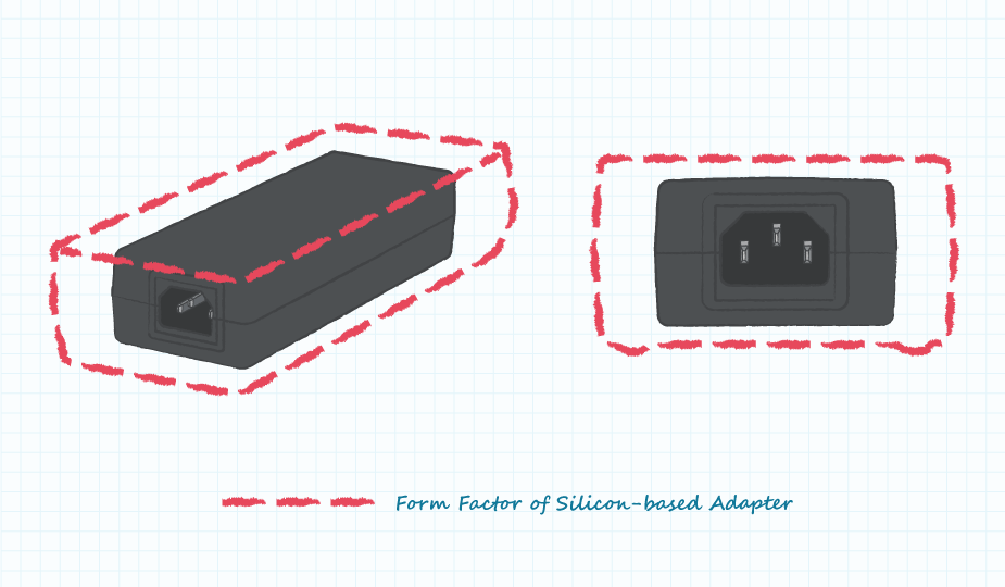 Figure 3: Comparison of Si based and GaN based adapter form factors. Photo: CUI
Improved efficiency, decreased size, and reduced weight have all been achieved, through the application of GaN, in CUI’s latest series of desktop adapters. For example, CUI’s SDI200G-U desktop adapter’s increased switching frequency has allowed its size to be reduced by more than half, increasing the power density from 5.3 W/in3 to 11.4 W/in3, which can be seen in Figure 3. This has also resulted in a weight reduction of 32% (820g to 560g). And by reducing conduction and switching losses, the adapters achieve efficiencies up to 95%. These GaN desktop adapters offer significant improvements to efficiency, size, and weight over conventional silicon-based supplies.
Figure 3: Comparison of Si based and GaN based adapter form factors. Photo: CUI
Improved efficiency, decreased size, and reduced weight have all been achieved, through the application of GaN, in CUI’s latest series of desktop adapters. For example, CUI’s SDI200G-U desktop adapter’s increased switching frequency has allowed its size to be reduced by more than half, increasing the power density from 5.3 W/in3 to 11.4 W/in3, which can be seen in Figure 3. This has also resulted in a weight reduction of 32% (820g to 560g). And by reducing conduction and switching losses, the adapters achieve efficiencies up to 95%. These GaN desktop adapters offer significant improvements to efficiency, size, and weight over conventional silicon-based supplies.
Editors' Pick: Insect-Sized Robot Takes Flight
Power supply manufacturers are always seeking ways to increase the efficiency and power density of their products. Many of the gains over the years have come from improvements to the silicon switches used inside the power supplies. But as silicon reaches its physical limits, manufacturers have had to look elsewhere for improvements. The use of GaN (with its lower losses and faster switching) allows manufacturers to push past the limitations of silicon and design smaller and more efficient power supplies while still leaving room to improve as GaN continues to develop. These improvements can be seen first-hand in CUI’s latest generation of GaN-based adapters.
Gallium Nitride (GaN) is a wide band-gap (WBG) semiconductor material, and like silicon, GaN can be used to make semiconductor devices such as diodes and transistors.
A power supply designer would choose a GaN transistor instead of silicon if they were targeting a small form factor and high efficiency. The losses in a silicon MOSFET make their use undesirable due to thermal management requirements, compared to a GaN transistor, which would dissipate less power and more efficiently conduct heat away.
Read More About: Nanomaterials Transform Manufacturing
The development of GaN transistors has been of particular interest to the power electronics industry. As a transistor, GaN shows significant advantages over silicon in critical areas that allow power supply manufacturers to significantly increase efficiency, while at the same time decreasing the size and weight of their devices.
How Does GaN Improve Efficiency?
Power transistors are one of the primary contributors to power loss in a switching power supply. Losses in the transistors are generally separated into two categories: conduction and switching. Conduction losses are those caused by current flow when the transistor is on, and switching losses occur in the transition between on and off states.
Figure 1: Theoretical limits of resistance between drain and source versus breakdown voltage for Si, GaN, and SiC transistors. Photo: CUI
In addition to improvements in conduction losses, the use of GaN also leads to a reduction in switching losses. Multiple factors contribute to switching losses, several of which are improved through the use of GaN. One loss mechanism results from the fact that the current in a FET begins to flow before the drain-source voltage begins to fall, as shown in Figure 2. During this time, the losses (equal to the volt-amp product) are very large. Increasing the speed at which the switch turns on will reduce the losses incurred during this transition. Because GaN transistors can turn on faster than silicon FETs, they are able to reduce the losses caused by this transition.
Figure 2: Drain Voltage and current waveforms during switching transition. Photo: CUI
Learn More About: Sensors Allow Robots to Feel Sensation
Because the body diode of a silicon transistor conducts during the dead-time, it must be turned off when the other switch turns on. During this time, current flows in the reverse direction as the diode turns off, causing additional losses. In a GaN transistor, the absence of a body diode results in near-zero reverse recovery losses.
How Does GaN Decrease Form Factor?
While switching losses occur in short periods within the switching period, it is useful to look at them averaged over time. While the losses during a single switching transition may be significant, if the time period between switches is large (meaning a low switching frequency), the average value can be kept at a safe level. Because the switching losses are lower in GaN, the time between switches can be reduced, increasing the switching frequency. The increased switching frequency allows the size of many large components (such as the transformer, inductors, and output capacitors) to be reduced.
GaN and other WBG devices also have better thermal conductivity and can withstand higher temperatures than silicon. Both help to reduce the need for thermal management components such as bulky heatsinks, frames, or fans. The absence of these devices (along with the shrinking of the powertrain components mentioned earlier) all lead to significant reductions in the overall size of the power supply.
GaN Desktop Power Adapters
Figure 3: Comparison of Si based and GaN based adapter form factors. Photo: CUI
Editors' Pick: Insect-Sized Robot Takes Flight
Power supply manufacturers are always seeking ways to increase the efficiency and power density of their products. Many of the gains over the years have come from improvements to the silicon switches used inside the power supplies. But as silicon reaches its physical limits, manufacturers have had to look elsewhere for improvements. The use of GaN (with its lower losses and faster switching) allows manufacturers to push past the limitations of silicon and design smaller and more efficient power supplies while still leaving room to improve as GaN continues to develop. These improvements can be seen first-hand in CUI’s latest generation of GaN-based adapters.
Related Content

Energy Blog: How Dangerous Are Gas-Powered Appliances?
Dec 12, 2024
Rewiring America study points to the benefits of switching away to clothes dryers, water heaters, and HVAC systems that use heat pumps.

Below and Beyond for Geothermal's Frontier
Dec 2, 2024
A new generation of startups is developing the drilling technology needed to reach rocks hot enough to provide clean, sustainable power whenever we need it.

Infographic: Shifting Sources for Electric Generation
Nov 26, 2024
Coal and gas dominate worldwide, though solar and wind power have made large gains in the past 23 years.

Novel Carbon Capture Tech Makes Case for More Wind Turbines
Nov 12, 2024
Wind turbines can be both sources of clean energy and a means of capturing carbon dioxide, thanks to a patented technology out of Purdue.