A Fungal Substrate for Sustainable Electronics
A Fungal Substrate for Sustainable Electronics
For a fast growing, biodegradable substrate for electronics, researchers are turning to mushrooms.
There’s something strange and inefficient about taking a lifeform, burying it underground for a 100 million years, then pumping it back out after it’s become oil, turning it into plastic and adding electronics for a few years’ use, and finally chucking it in the landfill where it will take another 500 years before it breaks down. It might make a lot more sense to use a material that doesn’t require eons to produce and half a millennium to decompose—but as a substrate for circuit boards, there are few things that beat plastic for low cost and rigidity.
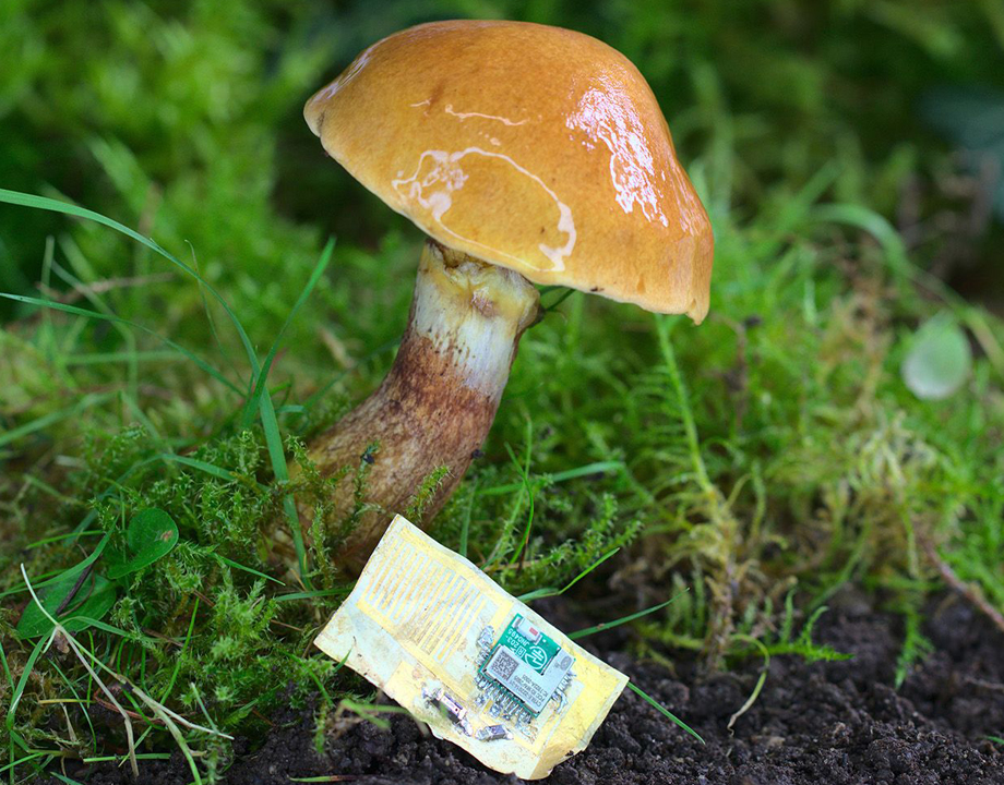
But now plastic as a base for electronics has competition: the mushroom. Researchers at the Johannes Kepler University in Linz, Austria, have used the Reishi mushroom (Ganoderma lucidum, to some), long cherished for its medicinal properties, to create a more sustainable, compostable, growable substrate.
They used the mycelium of the mushroom, the long white root-like strands that typically live underground or in rotting wood and pressed it into a paper-like material. “The fungus wants to protect its growth medium from the ingress of other bacteria and whatnot,” said Martin Kaltenbrunner, a professor of engineering, who heads the soft matter physics division and the Soft Materials Lab at the university, and co-author of the paper “MycelioTronics: Fungal mycelium skin for sustainable electronics,” which recently appeared in Science Advances. “They’re like a woven net, like a fabric, if you look at it under the microscope. It’s fluffy and it’s white and you can actually peel it off.”
Similar Reading: The Bionic Mushroom
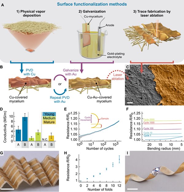
With a little fluffiness-reducing compression, the mycelium is made into thin sheets that can withstand temperatures of more than 480 °F, and don’t disintegrate or catch fire at higher temperatures. At the same time, they will break down with composting. And the shroomstrate’s flexibility can be calibrated by varying its thickness. They’re also amenable to laser engraving and electroplating. “This was not a given—for many materials you can very easily completely ruin your substrate with a laser,” said Kaltenbrunner. “The methods we have chosen are those that are convenient for us and didn't need too much extra engineering. And it's nice that the substrate is compatible with those.”
 Researchers at Johannes Kepler University in Linz, Austira, are taking the mycelium of mushrooms to create a more sustainable, compostable, growable substrate. Diagram: Johannes Kepler University
With these methods, Kaltenbrunner and his colleagues made a proximity sensor and a humidity sensor that could broadcast their readings via Bluetooth, as well as the batteries to power both. The mycelium film was also used as both the battery casing as well as a membrane to separate battery elements. “The major components of the battery itself are degradable,” said Kaltenbrunner.
Arguably the best thing about the new substrate is its ability to grow off a wide variety of sources that are usually discarded. Wood chips, straw, and other plant-based waste material can be mixed with the mushroom’s spores to grow the fungus, the mycelium of which is entirely ready for compression, without the need for additional processing. There’s no dearth to the amount of bio-material available for such exploitation: woods chips from industry and construction, and straw from growing rice, have little use and are usually tossed. Compared to paper, which requires a great deal of energy, water, and acids, to produce, the Reishi-sheets are far more environmentally friendly.
Become A Member: How to Join ASME
Plenty more work must be done before phones and laptops incorporate substantial quantities of MycelioTronics. “This was kind of the first step,” said Kaltenbrunner. “We need a bit more reproducibility right now.” He and his team are trying to find ways to grow more homogenous mycelium with larger growth areas, and to make them smoother to better process simple thin film electronic circuits.
Eventually, they plan to make multi-layered printed circuit boards. Right now, the circuits are built on only one side of the film. Kaltenbrunner hopes to eventually make a seven or eight layered stack, like the PCBs in modern computers. “Not sure if it’s entirely needed, but it’s a nice scientific challenge to see how far we can go,” he said. “If you really want to make an impact, you need to convince people that you can do more sophisticated electronics and replace state of the art circuit boards, eventually, with biodegradable versions.”
Michael Abrams is a technology writer based in Westfield, N.J.
But now plastic as a base for electronics has competition: the mushroom. Researchers at the Johannes Kepler University in Linz, Austria, have used the Reishi mushroom (Ganoderma lucidum, to some), long cherished for its medicinal properties, to create a more sustainable, compostable, growable substrate.
They used the mycelium of the mushroom, the long white root-like strands that typically live underground or in rotting wood and pressed it into a paper-like material. “The fungus wants to protect its growth medium from the ingress of other bacteria and whatnot,” said Martin Kaltenbrunner, a professor of engineering, who heads the soft matter physics division and the Soft Materials Lab at the university, and co-author of the paper “MycelioTronics: Fungal mycelium skin for sustainable electronics,” which recently appeared in Science Advances. “They’re like a woven net, like a fabric, if you look at it under the microscope. It’s fluffy and it’s white and you can actually peel it off.”
Similar Reading: The Bionic Mushroom
With a little fluffiness-reducing compression, the mycelium is made into thin sheets that can withstand temperatures of more than 480 °F, and don’t disintegrate or catch fire at higher temperatures. At the same time, they will break down with composting. And the shroomstrate’s flexibility can be calibrated by varying its thickness. They’re also amenable to laser engraving and electroplating. “This was not a given—for many materials you can very easily completely ruin your substrate with a laser,” said Kaltenbrunner. “The methods we have chosen are those that are convenient for us and didn't need too much extra engineering. And it's nice that the substrate is compatible with those.”
Researchers at Johannes Kepler University in Linz, Austira, are taking the mycelium of mushrooms to create a more sustainable, compostable, growable substrate. Diagram: Johannes Kepler University
With these methods, Kaltenbrunner and his colleagues made a proximity sensor and a humidity sensor that could broadcast their readings via Bluetooth, as well as the batteries to power both. The mycelium film was also used as both the battery casing as well as a membrane to separate battery elements. “The major components of the battery itself are degradable,” said Kaltenbrunner.
Arguably the best thing about the new substrate is its ability to grow off a wide variety of sources that are usually discarded. Wood chips, straw, and other plant-based waste material can be mixed with the mushroom’s spores to grow the fungus, the mycelium of which is entirely ready for compression, without the need for additional processing. There’s no dearth to the amount of bio-material available for such exploitation: woods chips from industry and construction, and straw from growing rice, have little use and are usually tossed. Compared to paper, which requires a great deal of energy, water, and acids, to produce, the Reishi-sheets are far more environmentally friendly.
Become A Member: How to Join ASME
Plenty more work must be done before phones and laptops incorporate substantial quantities of MycelioTronics. “This was kind of the first step,” said Kaltenbrunner. “We need a bit more reproducibility right now.” He and his team are trying to find ways to grow more homogenous mycelium with larger growth areas, and to make them smoother to better process simple thin film electronic circuits.
Eventually, they plan to make multi-layered printed circuit boards. Right now, the circuits are built on only one side of the film. Kaltenbrunner hopes to eventually make a seven or eight layered stack, like the PCBs in modern computers. “Not sure if it’s entirely needed, but it’s a nice scientific challenge to see how far we can go,” he said. “If you really want to make an impact, you need to convince people that you can do more sophisticated electronics and replace state of the art circuit boards, eventually, with biodegradable versions.”
Michael Abrams is a technology writer based in Westfield, N.J.
For a fast growing, biodegradable substrate for electronics, researchers are turning to mushrooms.
Related Content

Jul 8, 2025
Energy Blog: Coal’s Brightest Future May Not Be as a Fuel
For decades, a bipartisan consensus has tried to prop up the coal mining industry by supporting its use in the energy industry. Maybe they’ve been looking at coal the wrong way.

Jun 20, 2025
What Engineers Often Overlook About Glass Materials
Exploring the overlooked potential of borosilicate and glass ceramics in demanding applications.

Jun 12, 2025
These 5 Very Long Tunnels Are Engineering Marvels
Looking for the light at the end of the tunnel? You’ll have a long wait once you enter these underground passageways that extend farther than any others of their type.

Jun 6, 2025
A Night at the Gala: Engineering Edition
At the 2025 ASME Foundation Gala, engineering met imagination in a celebration of the leaders, innovators, and optimists of tomorrow.