Tunable Laser Platform Fits on a Fingertip
Tunable Laser Platform Fits on a Fingertip

Chip-scale laser system is a compact, cost-effective solution that could power high-impact technologies such as portable atomic clocks and AR/VR devices.
While working on visible-light integrated photonics projects at Columbia University, Mateus Corato Zanarella uncovered a consistent problem: a lack of tunable and narrow-linewidth laser sources across the visible spectrum to power and test his devices.
“In searching for a solution, I realized that I was not the only one with this problem. High-performance visible lasers are bulky and expensive, making it difficult for most research labs to have access to them,” said Zanarella, a sixth-year doctoral student in electrical engineering in Columbia Engineering’s Lipson Nanophotonics Group. He is lead author on the study, “Widely tunable and narrow-linewidth chip-scale lasers from near-ultraviolet to near-infrared wavelengths,” published in Nature Photonics in December.
Currently available visible lasers are benchtop units that are difficult to use outside research settings. But these types of lasers are necessary for high-impact applications such as quantum optics, optical clocks, atomic and molecular physics, displays for AR/VR, biosensors, and bioimaging, Zanarella explained. “In order to fulfill their potentials, they require narrow-linewidth, tunable visible lasers across the whole spectrum from near-ultraviolet to near-infrared,” he added.
Given the need for compact, inexpensive, and high-performance visible lasers, Zanarella and his team embraced integrated photonics in finding a solution.
“Until now, it’s been impossible to shrink and mass-deploy technologies that require tunable and narrow-linewidth visible lasers,” said Michal Lipson, Higgins Professor of Electrical Engineering and professor of applied physics, and a pioneer in silicon photonics, in a statement. “A notable example is quantum optics, which demands high-performance lasers of several colors in a single system. We expect that our findings will enable fully integrated visible light systems for existing and new technologies.”
You Might Also Enjoy: 7 Top Applications of Lasers in Manufacturing
The laser system is comprised of commercial Fabry-Perot (FP) laser diodes and a photonic integrated chip (PIC) that was designed to modify the laser emission through self-injection locking (SIL), which is a physical process of modifying the emission of a laser by reflecting a portion of its output light back to the laser cavity, Zanarella explained.
The PIC was also designed to purify the light that each laser diode emits. Combining the diode and the chip enables selective and controllable optical feedback, so the PIC forces the laser to emit a single color of high purity instead of multiple shades, he said.
“More specifically, a low-loss microring resonator-based feedback loop in our PIC selects a single wavelength and reflects a portion of its light back to the diode,” Zanarella added. “This selective optical feedback makes the chosen lasing mode win the competition for gain over all others, collapsing all the optical power of the laser to it and resulting in a single-frequency emission of narrow linewidth. By electrically controlling the microring resonator via on-chip phase shifters, we choose which lasing mode wins and consequently tune the wavelength of the emitted light.”
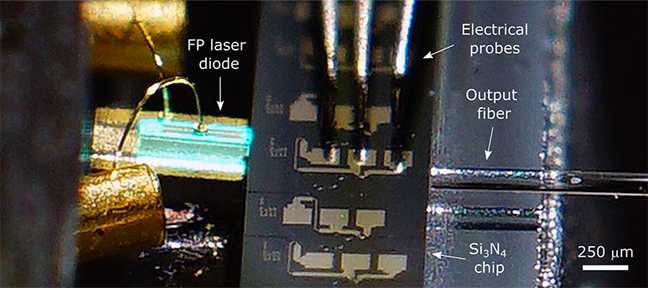 The Columbia team's laser system is comprised of commercial Fabry-Perot laser diodes and a photonic integrated chip that was designed to modify the laser emission through self-injection locking. Image: Columbia Engineering
While the chip-scale laser system remained mostly unchanged from initial concept, Zanarella did make improvements to the PIC design and experimental approaches. “The ‘ah-hah’ moment that proved that our idea would work was when I first saw indications of the wavelength collapse,” he said.
Initial design began in late 2019, while testing was pushed back until late 2020 due to the COVID-19 pandemic. Using those results, the team fabricated and tested a new generation of devices that were used for final testing.
“The biggest challenge we had to overcome was how to simultaneously mitigate the higher losses characteristics of integrated platforms at visible wavelengths and achieve robust broadband operation covering almost an octave,” Zanarella said. “At wavelengths shorter than red, the coupling and propagation losses of photonic integrated circuits increase significantly, which has prevented the realization of high-performance lasers at these colors.”
To solve the coupling loss problem, the team chose FP laser diodes as light sources, minimizing the impact of performance losses, he added. This offers lasers at record-short wavelengths while also providing scalability to high optical powers.
Become a Member: How to Join ASME
However, FP laser diodes emit several wavelengths of light simultaneously and are not easily tunable, despite being inexpensive and compact solid-state lasers. By combining them with the team’s specially designed PIC, laser emissions are modified to be single-frequency, narrow-linewidth, and widely tunable.
“We overcame the propagation loss issue by designing a platform that minimizes both the material absorption and surface scattering losses simultaneously for all the visible wavelengths,” Zanarella added. “To guide the light, we used silicon nitride, a dielectric widely used in the semiconductor industry that is transparent for visible light of all colors.”
Despite minimal absorption, light is still lost due to unavoidable roughness from the fabrication processes. “We solved this problem by designing a photonic circuit with a special type of ring resonator,” Zanarella said. “The ring has a variable width along its circumference, allowing for single-mode operation characteristic of narrow waveguides, and low loss characteristic of wide waveguides. The resulting photonic circuit provides a wavelength-selective optical feedback to the FP diodes that forces the laser to emit at a single desired wavelength with very narrow linewidth.”
The result is a robust and versatile platform that is scalable and works for all colors of light, he said.
It’s also a cost-effective solution. Currently available tunable and narrow linewidth lasers run in the tens of thousands of dollars, whereas the chip-scale lasers are in the tens of dollars. And even though the devices are dramatically smaller in scale as well, in terms of performance metrics, “our chip-scale lasers have tuning range, tuning speed, linewidth, power, and side-mode suppression ratio comparable to those state-of-the-art benchtop systems,” Zanarella noted.
More for You: 6 Ways 5G Will Impact Mechanical Engineering
The team has already filed a provisional patent for this technology.
“In order to move forward, we have to be able to miniaturize and scale these systems, enabling them to eventually be incorporated in mass-deployed technologies,” Lipson said. Work is progressing on further developing the optical and electrical packaging of the chip-scale lasers to turn them into standalone units for easy use in applications such as quantum optics, imaging, and sensing.
“One of the challenges left to overcome in this process is achieving packaging with low coupling loss between the laser diode and the PIC,” Zanarella said. “What I find most exciting moving forward is seeing our laser technology enabling and powering other high-impact technologies.”
Louise Poirier is senior editor.
“In searching for a solution, I realized that I was not the only one with this problem. High-performance visible lasers are bulky and expensive, making it difficult for most research labs to have access to them,” said Zanarella, a sixth-year doctoral student in electrical engineering in Columbia Engineering’s Lipson Nanophotonics Group. He is lead author on the study, “Widely tunable and narrow-linewidth chip-scale lasers from near-ultraviolet to near-infrared wavelengths,” published in Nature Photonics in December.
Currently available visible lasers are benchtop units that are difficult to use outside research settings. But these types of lasers are necessary for high-impact applications such as quantum optics, optical clocks, atomic and molecular physics, displays for AR/VR, biosensors, and bioimaging, Zanarella explained. “In order to fulfill their potentials, they require narrow-linewidth, tunable visible lasers across the whole spectrum from near-ultraviolet to near-infrared,” he added.
Given the need for compact, inexpensive, and high-performance visible lasers, Zanarella and his team embraced integrated photonics in finding a solution.
How it works
These “high-performance visible-light lasers” are small enough to fit on a fingertip and are capable of generating pure and controllable light of colors from near-ultraviolet to near-infrared. These are the first tunable and narrow linewidth chip-scale lasers for wavelengths shorter than red, featuring the smallest footprint and shortest wavelength of any other such lasers at 404 nm, Zanarella said. Colors of the lasers can be precisely tuned and they’re also fast, going up to 267 petahertz per second.“Until now, it’s been impossible to shrink and mass-deploy technologies that require tunable and narrow-linewidth visible lasers,” said Michal Lipson, Higgins Professor of Electrical Engineering and professor of applied physics, and a pioneer in silicon photonics, in a statement. “A notable example is quantum optics, which demands high-performance lasers of several colors in a single system. We expect that our findings will enable fully integrated visible light systems for existing and new technologies.”
You Might Also Enjoy: 7 Top Applications of Lasers in Manufacturing
The laser system is comprised of commercial Fabry-Perot (FP) laser diodes and a photonic integrated chip (PIC) that was designed to modify the laser emission through self-injection locking (SIL), which is a physical process of modifying the emission of a laser by reflecting a portion of its output light back to the laser cavity, Zanarella explained.
The PIC was also designed to purify the light that each laser diode emits. Combining the diode and the chip enables selective and controllable optical feedback, so the PIC forces the laser to emit a single color of high purity instead of multiple shades, he said.
“More specifically, a low-loss microring resonator-based feedback loop in our PIC selects a single wavelength and reflects a portion of its light back to the diode,” Zanarella added. “This selective optical feedback makes the chosen lasing mode win the competition for gain over all others, collapsing all the optical power of the laser to it and resulting in a single-frequency emission of narrow linewidth. By electrically controlling the microring resonator via on-chip phase shifters, we choose which lasing mode wins and consequently tune the wavelength of the emitted light.”
The Columbia team's laser system is comprised of commercial Fabry-Perot laser diodes and a photonic integrated chip that was designed to modify the laser emission through self-injection locking. Image: Columbia Engineering
While the chip-scale laser system remained mostly unchanged from initial concept, Zanarella did make improvements to the PIC design and experimental approaches. “The ‘ah-hah’ moment that proved that our idea would work was when I first saw indications of the wavelength collapse,” he said.
Initial design began in late 2019, while testing was pushed back until late 2020 due to the COVID-19 pandemic. Using those results, the team fabricated and tested a new generation of devices that were used for final testing.
“The biggest challenge we had to overcome was how to simultaneously mitigate the higher losses characteristics of integrated platforms at visible wavelengths and achieve robust broadband operation covering almost an octave,” Zanarella said. “At wavelengths shorter than red, the coupling and propagation losses of photonic integrated circuits increase significantly, which has prevented the realization of high-performance lasers at these colors.”
To solve the coupling loss problem, the team chose FP laser diodes as light sources, minimizing the impact of performance losses, he added. This offers lasers at record-short wavelengths while also providing scalability to high optical powers.
Become a Member: How to Join ASME
However, FP laser diodes emit several wavelengths of light simultaneously and are not easily tunable, despite being inexpensive and compact solid-state lasers. By combining them with the team’s specially designed PIC, laser emissions are modified to be single-frequency, narrow-linewidth, and widely tunable.
“We overcame the propagation loss issue by designing a platform that minimizes both the material absorption and surface scattering losses simultaneously for all the visible wavelengths,” Zanarella added. “To guide the light, we used silicon nitride, a dielectric widely used in the semiconductor industry that is transparent for visible light of all colors.”
Despite minimal absorption, light is still lost due to unavoidable roughness from the fabrication processes. “We solved this problem by designing a photonic circuit with a special type of ring resonator,” Zanarella said. “The ring has a variable width along its circumference, allowing for single-mode operation characteristic of narrow waveguides, and low loss characteristic of wide waveguides. The resulting photonic circuit provides a wavelength-selective optical feedback to the FP diodes that forces the laser to emit at a single desired wavelength with very narrow linewidth.”
The result is a robust and versatile platform that is scalable and works for all colors of light, he said.
Economical solution
The Columbia team’s chip-scale lasers have performance metrics such as tuning range, tuning speed, linewidth, power, and side-mode suppression ratio previously only possible with expensive benchtop laser systems, Zanarella said. “This opens the doors for high-end applications such as portable atomic clocks that were previously not possible due to the size of the required laser sources."It’s also a cost-effective solution. Currently available tunable and narrow linewidth lasers run in the tens of thousands of dollars, whereas the chip-scale lasers are in the tens of dollars. And even though the devices are dramatically smaller in scale as well, in terms of performance metrics, “our chip-scale lasers have tuning range, tuning speed, linewidth, power, and side-mode suppression ratio comparable to those state-of-the-art benchtop systems,” Zanarella noted.
More for You: 6 Ways 5G Will Impact Mechanical Engineering
The team has already filed a provisional patent for this technology.
“In order to move forward, we have to be able to miniaturize and scale these systems, enabling them to eventually be incorporated in mass-deployed technologies,” Lipson said. Work is progressing on further developing the optical and electrical packaging of the chip-scale lasers to turn them into standalone units for easy use in applications such as quantum optics, imaging, and sensing.
“One of the challenges left to overcome in this process is achieving packaging with low coupling loss between the laser diode and the PIC,” Zanarella said. “What I find most exciting moving forward is seeing our laser technology enabling and powering other high-impact technologies.”
Louise Poirier is senior editor.
Related Content

Fulfilling a Dream: The Late-in-Life Ph.D.
Apr 16, 2024
The trend of pursuing a Ph.D. later in life is real. But there are challenges for students who decide to return to the classroom and pursue an advanced degree.

Breakthrough Could Make for Long-Range EVs
Apr 16, 2024
A simple method could lead to electric vehicles that can go much father on a single charge, and batteries that last years longer than present technology.

Mapping 2D Ferroelectric Materials Unveils Connections
Apr 15, 2024
Identifying structural features of 2D ferroelectric materials could influence the design of next generation nanoelectronics.

Aircraft Carriers May Get Advanced Hoist
Apr 15, 2024
To streamline operations and improve performance, the U.S. Navy commissioned a new hoist to raise and lower the aircraft elevators.